A metasurface the size of a pinhead could finally unlock one of the electromagnetic spectrum's most stubborn blind spots. Researchers at Cambridge and Swansea universities have engineered a quantum terahertz detector that concentrates radiation into active regions with a repeating brickwork pattern, sidestepping decades of limitations that have made this invisible part of the spectrum so difficult to measure.
Terahertz light sits in an awkward middle ground—too high-energy for conventional microwave detectors, too low for infrared sensors. For years, capturing these frequencies has required bulky equipment, extreme cryogenic cooling, and detectors that simply miss most of the incoming radiation. The gap has left applications like medical imaging, security scanning, and materials analysis starved of practical tools. Now, Wladislaw Michailow and his team have solved a fundamental bottleneck by weaving quantum physics directly into a metasurface.
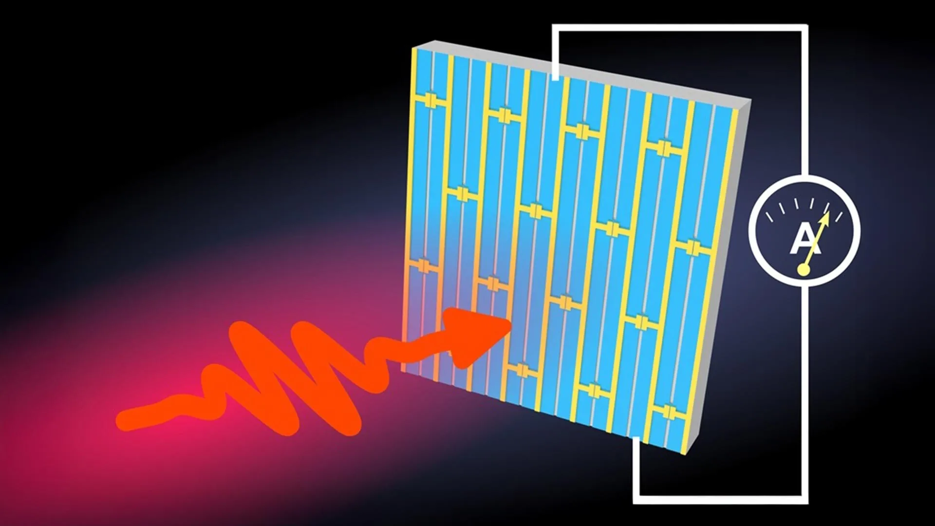
The breakthrough hinges on a quantum phenomenon called the in-plane photoelectric effect. When terahertz photons strike the device, they transfer energy to electrons confined within a two-dimensional electron gas layer. These energized electrons cross a carefully engineered potential step, producing a measurable electrical current. Unlike conventional photoelectric detectors, this process requires no minimum photon energy threshold and avoids efficiency losses that plagued earlier designs. But the real innovation is architectural. Rather than relying on isolated antenna elements that capture only fragments of incoming radiation, Michailow's team embedded detection elements directly into the capacitive gaps of a metasurface. The brickwork pattern acts as a concentrator, funneling terahertz energy into narrow regions where the electric field is strongest—precisely where the conversion to electrical signal happens.
"This ensures optimal coupling of the metasurface to the detection elements," Michailow explains. "Compared to the conventional approach of connecting multiple devices in parallel, this approach allowed us to significantly boost the detection sensitivity."
The team used computer simulations to fine-tune every structural detail: gap dimensions, spacing between repeating units, and the electron channel width. Each parameter was optimized to maximize both field enhancement and measurable output. When the researchers tested the device at 10 Kelvin, exposed to radiation at 1.9 terahertz, it responded with a clear electrical signal that precisely mirrored the on-off modulation of the incoming beam. The responsivity reached 2.7 amperes per watt—impressive for any detector, but especially for one operating at zero source-drain bias, which eliminates the noise that plagues many competing designs.
The numbers tell a striking story: the external quantum efficiency hit 2.1 percent, roughly twenty times better than previous in-plane photoelectric detectors. That leap comes directly from the metasurface's ability to capture a much larger fraction of incoming radiation and focus it into active regions. Because the metasurface itself concentrates the light, external optics like silicon lenses become unnecessary, dramatically simplifying assembly.
Manufacturing fits squarely within existing semiconductor infrastructure—the fabrication process mirrors techniques already used for field-effect transistors. That compatibility suggests a practical pathway to integration with real electronics and, eventually, mass production. The proof-of-concept is compact, semiconductor-friendly, and operates without the complex cooling and external optical systems that have held terahertz detection back. For researchers and engineers waiting for terahertz to become accessible, the gap just got a lot narrower.