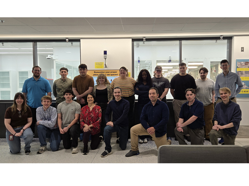
When Cari Caudill walked into MIT.nano's cleanroom for the first time, she wasn't just visiting a lab—she was stepping into a world most community college students never see up close. "I found the combination of hands-on activities, lectures, and informal discussion with the MIT.nano team and fellow students fostered an awesome learning environment," said Caudill, a mechanical engineering student at North Shore Community College. For two days in May, she and eleven other students from across the Northeast learned to build functional photonic chips using the same advanced tools used by industry professionals.
The boot camp, held May 20-21, brought together students from MassBay Community College, North Shore Community College, Stonehill College, and SUNY Polytechnic Institute to the fifth floor of MIT.nano in Cambridge, Massachusetts. Under the guidance of principal research scientist Anu Agarwal and her Lab for Education and Application Prototypes (LEAP) team, the students operated industrial-grade equipment including a die saw, die bonder, wire bonder, and flip chip tool—machines that cost millions and require specialized training to run. By the end of the two days, they had built and tested their own packaged chips.
The program is called NCAIST—the Northeast Consortia for Advanced Integrated Silicon Technologies—and its mission goes far beyond a single workshop. Coordinated with AIM Photonics, a U.S. Manufacturing Innovation Institute, NCAIST bridges the gap between cutting-edge semiconductor research and the broader educational pipeline. "Having a workforce skilled in resource-efficient semiconductor manufacturing, including electronic-photonic packaging, is critical to maintain the exponential growth of the chip industry and build national security," said Agarwal.
Marina Bograd, professor and chair of the engineering department at MassBay Community College, has seen the boot camp transform her students. "For many of them, this is their first time stepping into a cleanroom or seeing semiconductor manufacturing up close," she said. "The experience helps open doors that might otherwise feel out of reach, builds confidence, and inspires our students to see themselves pursuing careers in emerging technologies."
The curriculum combined physical fabrication with virtual reality simulations developed by Sajan Saini, director of education at the Initiative for Knowledge and Innovation in Manufacturing (IKIM). Students received lectures on cleanroom safety from Kristofer Payer, electronic-photonic packaging from Agarwal, and photonic integrated circuit sensing from graduate student Lizzie Gower. The VR exercises helped them visualize photonic devices and complex tool mechanics before touching the real equipment.
MassBay student Wyatt Maurer called the experience "exciting and illuminating." "I really appreciated getting the chance to work with semiconductor manufacturing tools and to learn about the future of photonics from leaders in the field," he said. Agarwal stressed that there is currently no standardized university curriculum for integrated electronics-photonics packaging—a gap NCAIST and MIT.nano are working to fill by training students at every level, from community college to graduate school. "MIT.nano, through programs like NCAIST, are helping to train more people in STEM," she said, "and the experience at this boot camp not only strengthens our students' technical skills, it helps them see themselves as future contributors to a rapidly evolving field."